
Scanning Electron Microscope (SEM) with EDS
High-resolution imaging and elemental analysis of material surfaces.
Overview
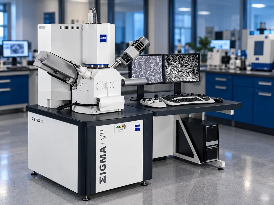
The Zeiss Sigma is a field-emission scanning electron microscope with energy dispersive X-ray spectroscopy (EDS). It images surface detail at high magnification and identifies the elements present in a selected area.
Applications
- Material surface analysis
- Elemental composition and element mapping (EDS)
- Fractography
- Microstructure examination
Technical Specifications
- Make
- Zeiss
- Model
- Sigma
- Electron source
- Schottky thermal field emitter
- Accelerating voltage range
- 0.2 to 30 kV
- Current range
- 4 pA to 20 nA
- Variable pressure range
- 2 – 133 Pa
- Detectors
- In-lens secondary electron, Everhart-Thornley secondary electron, variable pressure secondary electron, backscattered electron
- Resolution at 1 kV / 15 kV
- 2.8 nm / 1.5 nm
- Maximum image size
- 3072 × 2304 pixels
- Sample chamber
- Specimens up to 250 mm diameter and 45 mm tall
- EDS detector
- 80 mm² silicon-drift detector
Specifications are as stated in the instrument documentation.
Category
Microscopy
Related Testing Services
Have a Material Testing Requirement?
Tell us about your sample and testing objective, and our team will help you decide the appropriate next step.